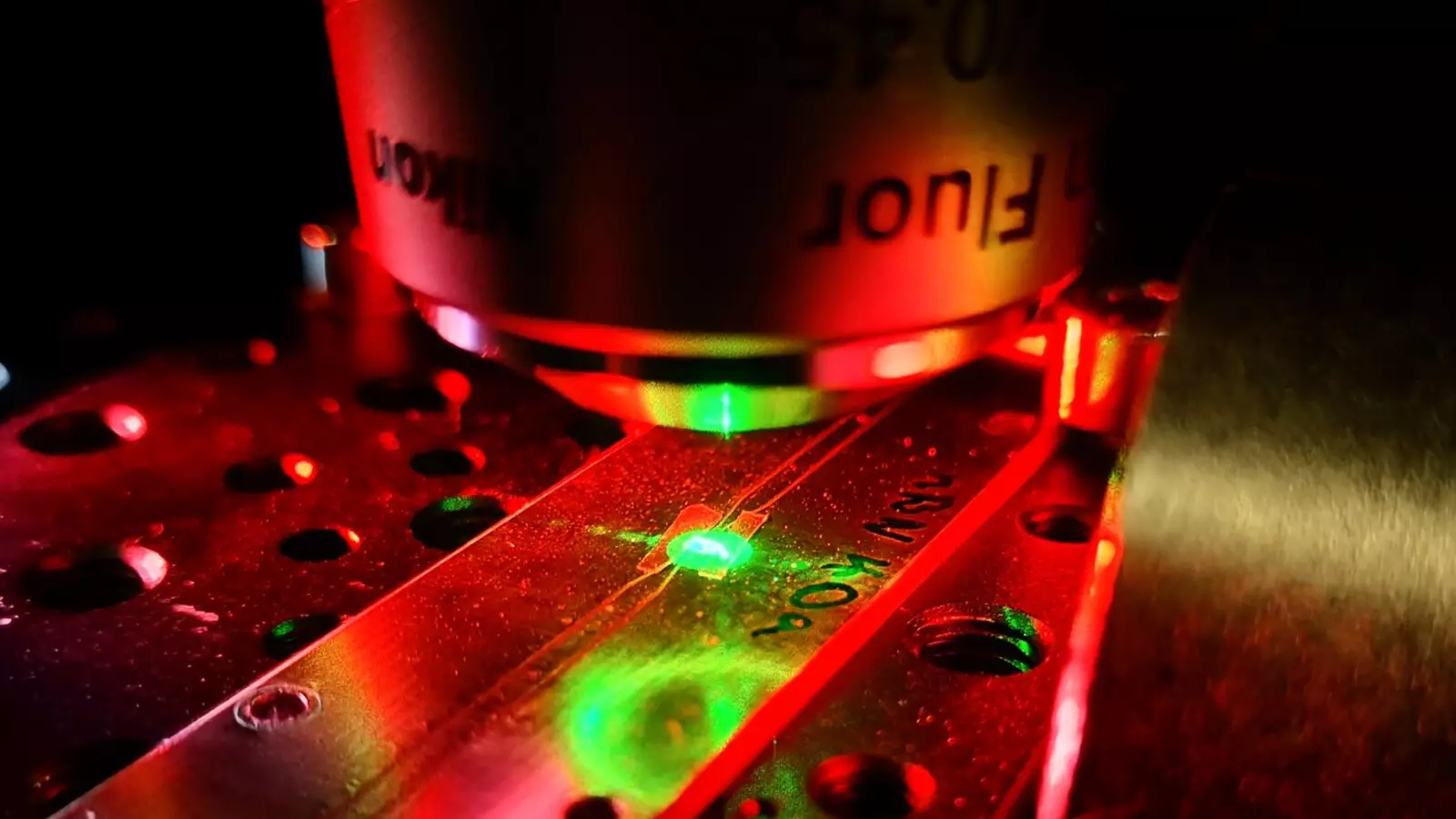
In a groundbreaking development, researchers at TMOS, along with collaborators at RMIT University, have introduced a novel 2D quantum sensing chip that utilizes hexagonal boron nitride (hBN) to detect temperature anomalies and magnetic fields in any direction. This thin-film sensor represents a significant advancement in quantum technology, offering a more versatile and cost-effective alternative to existing magnetometry systems.
Traditionally, quantum sensing chips have been constructed using diamond due to its durability and stability. However, diamond-based sensors are limited in their ability to detect magnetic fields unless perfectly aligned with the field direction. This constraint results in blind spots and necessitates the use of multiple sensors at various alignments, making operation complex and limiting the sensor’s applicability across different scenarios.
The research team led by TMOS Associate Investigator Jean-Philippe Tetienne and Chief Investigator Igor Aharonovich is pioneering a new frontier in quantum sensing by leveraging the unique properties of hBN. Unlike diamond, hBN crystals consist of atomically thin layers that offer flexibility, allowing the sensor to conform to the sample’s shape and achieve closer proximity, thereby enhancing sensitivity and accuracy.
Through rigorous experimentation, the team uncovered a carbon-based defect within hBN that exhibits half spin behavior, enabling it to detect magnetic fields in any orientation. By comparing this newly identified defect with the well-understood boron vacancy defect in hBN, the researchers confirmed its spin half nature and established its potential for magnetic field sensing.
Encouraged by their findings, the team proceeded to develop a hBN sensing chip that harnesses both spin defects simultaneously to measure magnetic fields and temperature. This innovative approach resulted in the first-ever magnetic images captured using the isotropic sensor, marking a significant milestone in quantum sensing research.
The unique 2D structure of hBN holds promise for a wide range of applications, including in-field identification of magnetic geological features and radio spectroscopy across a broader range. The cost-effectiveness and accessibility of hBN further enhance its appeal as a quantum sensing material, offering a viable alternative to diamond in various applications.
As the research progresses, the team aims to identify and characterize additional atomic defects within hBN to further enhance sensor performance. By leveraging the properties of these defects, they seek to optimize sensor devices for improved functionality and expanded capabilities, paving the way for new opportunities in optical spin defect exploration.


Leave a Reply