Recent advancements in semiconductor research have opened up new avenues for understanding the fundamental processes that govern electronic devices. At the forefront of this exploration are researchers from UC Santa Barbara, who have achieved a significant milestone by creating the first visual representation of electric charges as they travel across the interface of different semiconductor materials. This development not only enhances our comprehension of semiconductor behavior but also establishes a new framework for evaluating existing theories and measurements in the field.
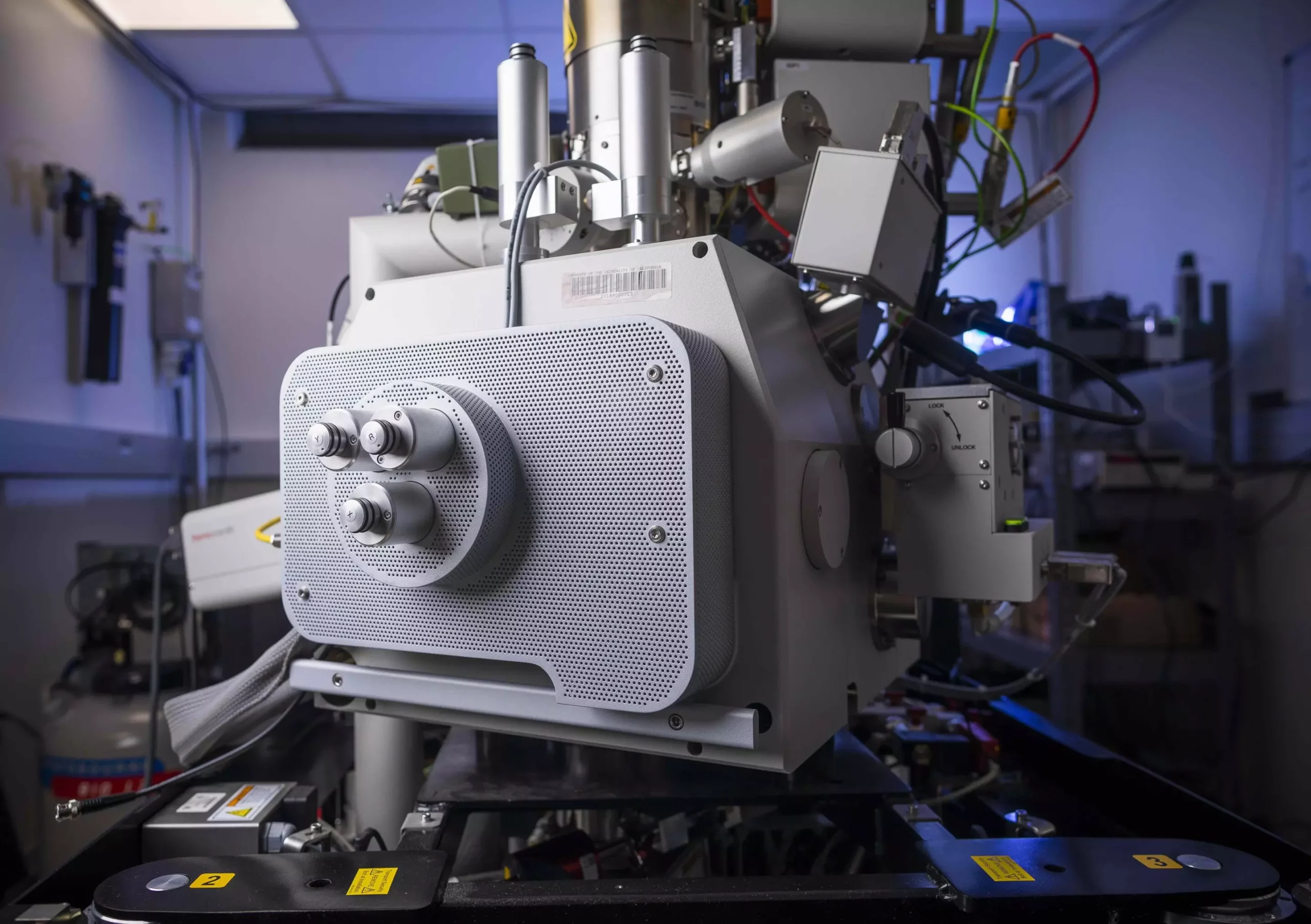
The breakthrough stems from the innovative scanning ultrafast electron microscopy (SUEM) techniques developed in the Bolin Liao lab. This method significantly improves our ability to study transient electronic events by allowing researchers to visualize how charge carriers—specifically photocarriers—behave in real-time. “There are many textbooks discussing this phenomenon, yet most existing data come from indirect measurements,” notes Bolin Liao, an associate professor of mechanical engineering. By utilizing SUEM, the team has not just improved measurement accuracy but has also provided direct visualization of processes that previously eluded scientists.
This novel imaging approach employs ultrafast laser pulses to create a shutter effect that captures events occurring within a time window of picoseconds to nanoseconds. When combined with an electron beam, this technique offers a dynamic view of how photocarriers traverse the junction between two semiconductor materials—an essential component for applications such as solar cells and lasers.
Understanding Photocarriers and Their Dynamics
Photocarriers are generated when light interacts with semiconductor materials, exciting electrons to higher energy states and allowing them to move freely. This excitation process also creates ‘holes’—the absence of electrons—leading to the generation of electric current. However, a notable challenge arises from the fact that these carriers typically lose most of their energy within picoseconds. The energy harvested by conventional photovoltaic systems is merely a fraction of what the carriers possess in their “hot” state before they return to thermal equilibrium and dissipate energy as heat.
The ability to visualize the movement of these hot carriers across semiconductor interfaces is vital. Through their research, Liao and his team specifically examined the heterojunction created from silicon and germanium, materials widely utilized in solar energy and telecommunications. Understanding how charge carriers behave at this critical junction allows researchers to identify and address potential inefficiencies in semiconductor devices.
The ability to directly observe the diffusion of photocarriers across the heterojunction provided several insights. As Liao elaborates, when charges are excited in uniform regions like silicon or germanium, they exhibit high mobility initially, exhibiting swift movement due to their elevated energy state. However, when these charges are generated near the junction itself, some of them become trapped due to the energy potential barrier at the interface. This trapping phenomenon significantly impedes carrier mobility, which poses a risk to the overall efficiency of devices relying on these hot charges.
The recognition that such events can now be visually imaged is pivotal. Liao expressed his surprise at being able to capture this effect directly, a feat previously deemed impractical. It underscores the practical applicability of SUEM in advancing our understanding of semiconductor fundamentals.
This research opens new avenues for semiconductor scientists and engineers, particularly in designing and optimizing devices that rely on photocarrier separation and collection. Understanding the challenges presented by charge trapping, especially at heterojunctions, can lead to improvements in device architectures and potentially enhance the performance of photovoltaics, lasers, and other semiconductor applications.
Moreover, this study is a culmination of decades of evolution within semiconductor research, stemming from the pioneering ideas of Herbert Kroemer. His assertion that “the interface is the device” has guided the development of heterostructures which are crucial to modern electronics. As we continue to unveil the intricacies of charge dynamics, future innovations may further bridge the gap between theory and practice in semiconductor technology.
The research conducted at UC Santa Barbara marks a significant leap in semiconductor science, allowing us to visualize charge carrier behavior in unprecedented detail. By fostering a deeper understanding of how these carriers operate at heterojunctions, researchers are well-positioned to tackle current challenges in energy efficiency and electronic performance. As we move forward, this discovery serves as both a validation of theoretical frameworks and an impetus for future innovation in semiconductor technology.
Leave a Reply