Recent research from the University of Chicago has ushered in a new era for material science, particularly in understanding antiferroelectric materials. These intriguing substances, characterized by their unique electrical properties, present dramatic potential for applications like energy storage, sensors, and advanced memory devices. However, the need for deeper knowledge about these materials has faced several barriers, primarily due to the limitations of current imaging technologies. This breakthrough research shines a spotlight on how addressing these challenges can not only extend our grasp of physics but also propel next-generation technologies.
Antiferroelectric materials are particularly fascinating due to their unique arrangement of electric dipoles, which, instead of contributing to net polarization, effectively cancel each other out. This property creates an electrically neutral state under normal conditions, but the potential for switching to a high-energy state opens up a world of possibilities. As such, comprehending these materials is imperative for capitalizing on their electrifying capabilities—especially in efficiency-demanding applications like electronics and energy systems.
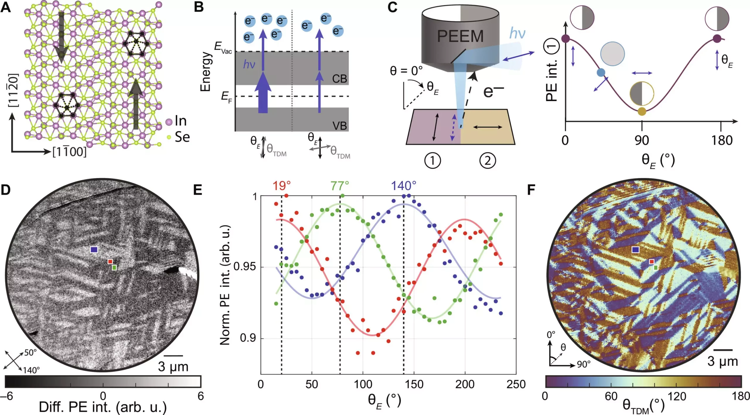
Novel Imaging Techniques Transforming Research
The research led by Assistant Professor Sarah King marks a significant advancement in the analysis of antiferroelectric materials. The team’s pioneering work in electron microscopy has heralded a method that allows for unprecedented visualization of these materials at the nanoscale. Traditional imaging methods have often faltered in their ability to discern the subtleties involved in the electrical properties of these materials, leading to substantial knowledge gaps in critical areas of research.
King’s team highlighted the challenge of visualizing antiferroelectric domain structures, which directly influence the material’s characteristics. Previously, researchers struggled to determine whether a material was antiferroelectric due to inadequate visualization techniques. By successfully utilizing polarization-dependent photoemission electron microscopy, the researchers have navigated around this challenge. This innovative approach combines polarized laser light and electron imaging, paving the way for a more holistic understanding of the orientation and arrangement of antiferroelectric domains.
Mapping the Invisible
One of the most exciting aspects of this advancement is how it enables scientists to “map” the invisible structures of antiferroelectric materials. The ability to observe and characterize these domains yields insights into their dynamics and helps optimize their configurations for various applications. In particular, the team focused on indium selenide, a commonly used material that has drawn attention for its promising applications.
In an arena where understanding the arrangement of atomic structures can dictate material performance, King’s breakthrough offers direct access to the intricate dance of electric dipoles within these materials. Such insights promise not just a better understanding of how to manipulate these materials but also invigorate other fields overlapping with material science, leading to enhanced innovations.
Future Implications and Production Possibilities
The significance of King’s findings cannot be overstated. By combining advanced imaging techniques with newfound insights into antiferroelectric domain dynamics, researchers can now envision a future where the potential of these materials is fully harnessed. This prepares the ground for engineers and scientists to develop more efficient electronic devices, robust energy storage systems, and sensitive sensors.
Moreover, there’s a prevailing curiosity within King’s team regarding the interactions among different material properties and how they culminate in organized states. This emphasis on order and hierarchy may illuminate paths not only for antiferroelectric materials but also for related fields of research, particularly ferroelectric materials.
As the world’s reliance on advanced technology continues to ebb and flow, understanding these materials offers not just a scientific achievement but a tangible step toward sustainability and optimization in technology. The future of energy-efficient devices and responsive sensors hinges on our comprehension of these intricate materials, and thanks to King’s innovative work, the barriers to their understanding may soon be a thing of the past.
The enthusiasm surrounding this research is palpable among the collaborative team, which includes a vibrant mix of graduate and undergraduate students, researchers, and experts from institutions like Oak Ridge National Laboratory. This collaborative spirit signifies that the breakthroughs in material science are not isolated phenomena but rather collective efforts that can shape the future landscape of technology and sustainability.
Leave a Reply