In a groundbreaking endeavor, researchers from the Department of Energy’s Lawrence Berkeley National Laboratory (Berkeley Lab) have unveiled an innovative strategy to discover materials that could transform quantum technologies. Recognized for its potential in quantum computing, telecommunications, and sensing, this new approach leverages advanced computational methods to sift through a myriad of materials, rapidly identifying which ones hold the most promise for quantum applications. By using high-throughput computational techniques combined with atomic-scale fabrication, the research team, which includes members from prestigious institutions like Dartmouth College and the University of California, has set the stage for what could be a quantum revolution.
The Quest for Quantum Defects
The study, published in *Nature Communications*, highlights how theoretical predictions can guide experimental efforts, thereby flip-flopping traditional research paradigms that often rely on serendipity for discovering functional quantum defects. In quantum information science, defects in materials play a pivotal role, as their electronic properties must be finely tuned to enable applications. The researchers emphasize that the ideal defects should possess specific electronic structures to efficiently absorb and emit light in the visible and telecommunications range—properties that can fundamentally alter the landscape of quantum applications.
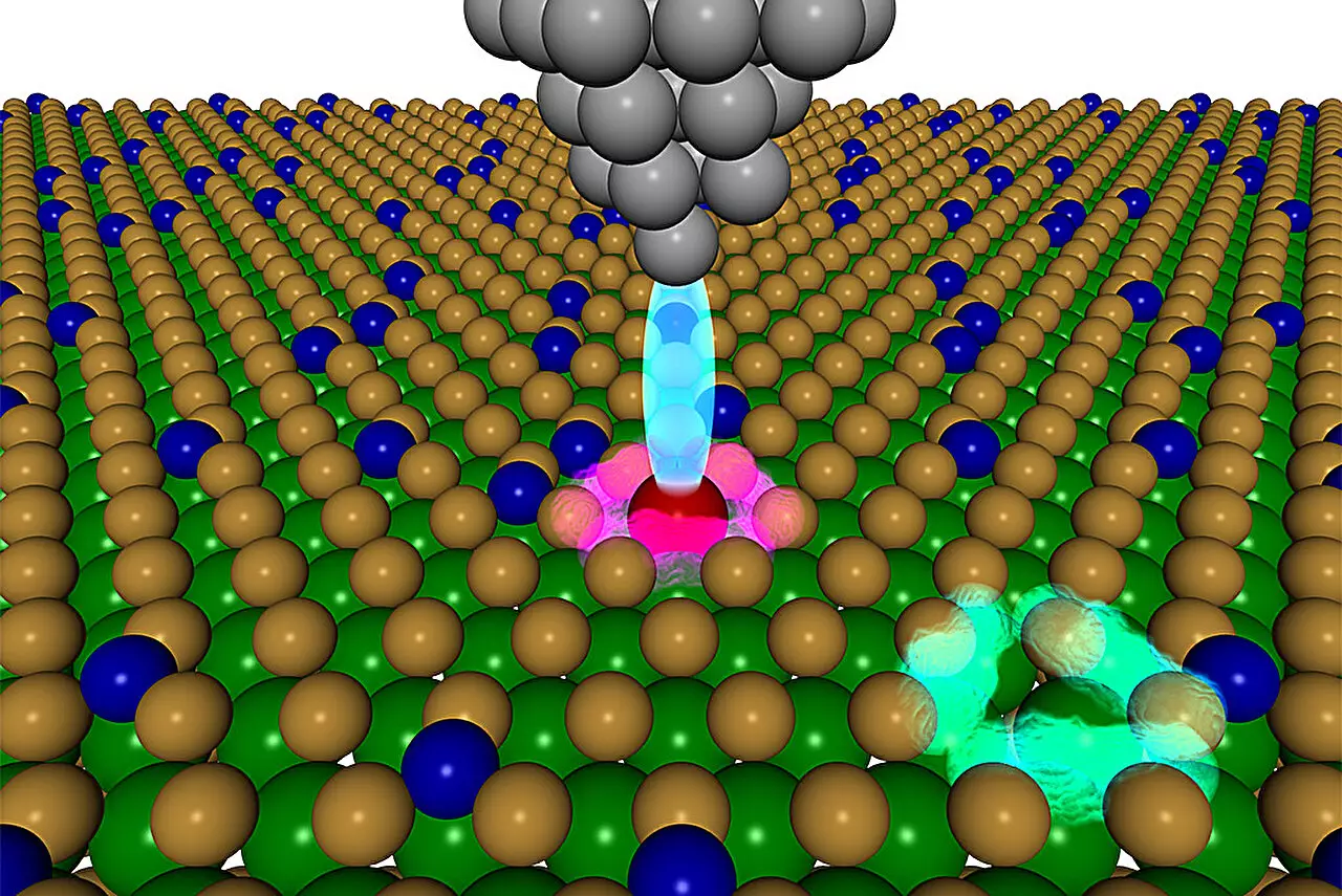
The team rigorously examined two-dimensional (2D) materials, specifically tungsten disulfide (WS2), which are notably compact—just one atom thick. The challenge, however, lies in the vast array of potential defects. With the possibility of substituting atoms and placing a myriad of elements within WS2, the researchers face a combinatorial explosion in the number of potential defects—hundreds of thousands even—making a traditional ‘trial and error’ approach impractical.
Shifting Paradigms: The Role of Advanced Computation
Traditionally, the journey to discovering functional quantum defects involved laborious experimentation. Researchers would fabricate and evaluate one defect at a time, leading to a time-consuming process that could stretch over decades. This research team revolutionized that approach, utilizing high-throughput computational methods to efficiently screen over 750 potential defects within WS2. By predicting essential properties such as stability and electronic configurations, they significantly narrowed down the options for experimental verification.
The team, which includes specialists from Dartmouth and Université Catholique de Louvain, created an efficient pipeline that first screened defects computationally before transitioning to laboratory work. This shift not only saves time but also increases the likelihood of discovering defects with ideal quantum characteristics.
Precision Fabrication: Crafting the Future
After identifying promising defects through computational analysis, the next challenging feat was precise fabrication. The researchers adeptly utilized a new technique at the Molecular Foundry, where they engineered atomic-level control over defect positioning. By manipulating a WS2 sample using argon ions to create vacancies and then strategically placing cobalt atoms into those vacancies with a scanning tunneling microscope, the team achieved unprecedented control.
John Thomas, one of the postdoctoral researchers, articulated the accomplishment with enthusiasm, noting that such precision allows scientists to conduct the equivalent of atomic-level construction, akin to playing with LEGO bricks. The importance of creating identical defects cannot be overstated, as the ability for defects to interact is crucial for their application in quantum communication.
The Innovative Collaboration that Fuels Progress
Integral to this study’s success was the close collaboration between theorists and experimentalists. The team emphasized the significance of teamwork, continuous feedback, and a unified funding source that kept everyone aligned on their common goal. This collaborative environment fosters innovation and fluid dialogue, essential components for enhancing research quality.
This model could become a paradigm for future investigations in quantum material research. By cultivating an environment where computational and experimental efforts are intrinsically linked, teams can effectively navigate the complexities of material science, pushing the envelope further than ever before.
The Future of Quantum Materials: Endless Possibilities
The researchers intend to explore more potential quantum defects and investigate how to make improvements on the cobalt defect’s properties. This endeavor is not just about these materials’ current functionalities; it’s about unlocking future capabilities that remain unknown. The ability to control defects with atomic precision suggests that we might soon engineer materials that possess entirely new functionalities, paving the way for advancements in quantum states resistant to disturbances in their environment.
As Weber-Bargioni aptly noted, this innovative intersection of computing and fabrication provides a thrilling glimpse into a future where material functionalities exceed our current imagination—just the tip of the iceberg in the pursuit of breakthrough quantum applications. The ramifications could profoundly reshape not only quantum technology, but also our understanding of material science itself.
Leave a Reply