The exploration of two-dimensional materials has opened up a realm of possibilities for scientists seeking to understand the unique properties these materials exhibit. When a material is reduced to just one or two layers of molecules, it undergoes a remarkable transformation. This transformation results in the material displaying completely different characteristics compared to its thicker counterparts.
A team of researchers led by physicist Prof. Ursula Wurstbauer from the University of Münster has been delving into the realm of two-dimensional crystals to investigate how their properties can be controlled. The goal is to manipulate these materials to behave as insulators, electrical conductors, superconductors, or even ferromagnets. By focusing on the interactions between charge carriers (electrons) and the energy landscape of the crystals, the team aims to unlock the potential of these materials.
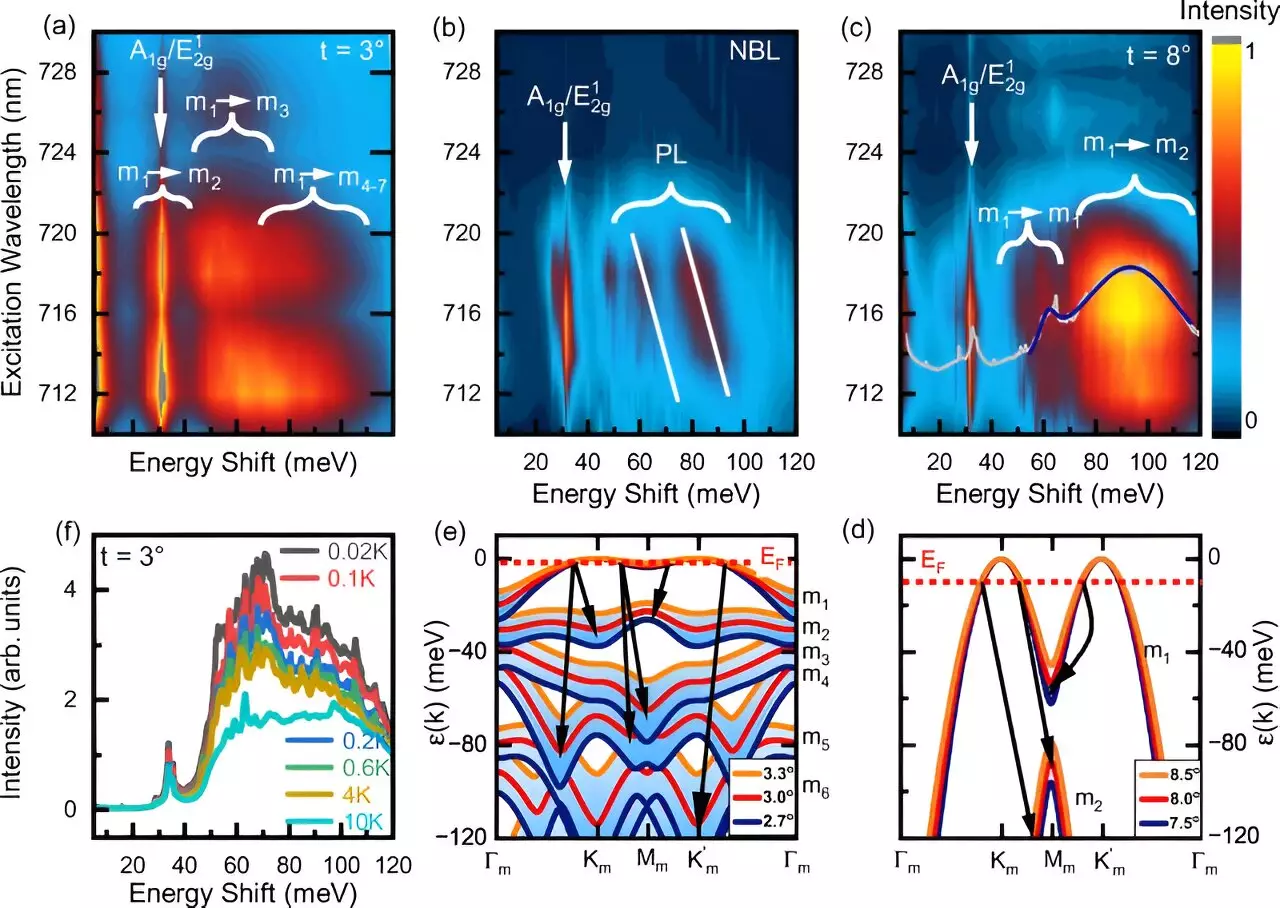
The groundbreaking study published in Physical Review Letters marks a significant advancement in our understanding of the electronic characteristics of crystal structures. The research team has successfully generated and quantitatively demonstrated collective excitations of charge carriers within various energy landscapes. This breakthrough sheds light on ways to influence the properties of these materials and harness their unique features for innovative applications.
One of the key strategies employed by the scientists involved placing two layers of a two-dimensional crystal on top of each other and slightly twisting them. This twisting action creates intricate geometric patterns known as moiré patterns, reminiscent of layers of thin curtain fabric overlapping. These patterns define the energy landscape of the material and result in slowed electron movement. As a result, electrons interact more intensely with each other, leading to what is known as strongly correlated behavior.
The implications of these findings extend beyond basic research, as they offer promising opportunities in quantum technology and the development of neuromorphic components and circuits. The ability to manipulate the properties of two-dimensional crystals opens up new avenues for innovation and the creation of cutting-edge technologies.
The collaborative effort of the research team, which included scientists from various institutions such as the University of Hamburg, RWTH Aachen University, and the Max Planck Institute for the Structure and Dynamics of Matter in Hamburg, demonstrates the interdisciplinary nature of this research. By combining experimental work with theoretical analyses, the team was able to gain valuable insights into the behavior of different two-dimensional crystals, including graphene, molybdenum diselenide, and tungsten diselenide. Utilizing optical spectroscopy methods at cryogenic temperatures, such as resonant inelastic light scattering spectroscopy, enabled the researchers to explore the intricate properties of these materials in depth.


Leave a Reply