The realm of electronics engineering and materials science has been on a constant quest to discover materials that can push the boundaries of electronic performance beyond the constraints imposed by silicon-based transistors. Among the various materials being explored, two-dimensional (2D) semiconductors have emerged as highly promising candidates. Their atomically thin structure and high carrier mobilities offer the potential to enhance the electrostatic control and ON-state performances of field-effect transistors (FETs).
Despite the numerous advantages offered by 2D semiconductors, they are not without their challenges. High contact resistances, often associated with Fermi-level-pinning effects, have hindered their performance in transistors. This key limitation has prevented the widespread adoption of these materials in electronics.
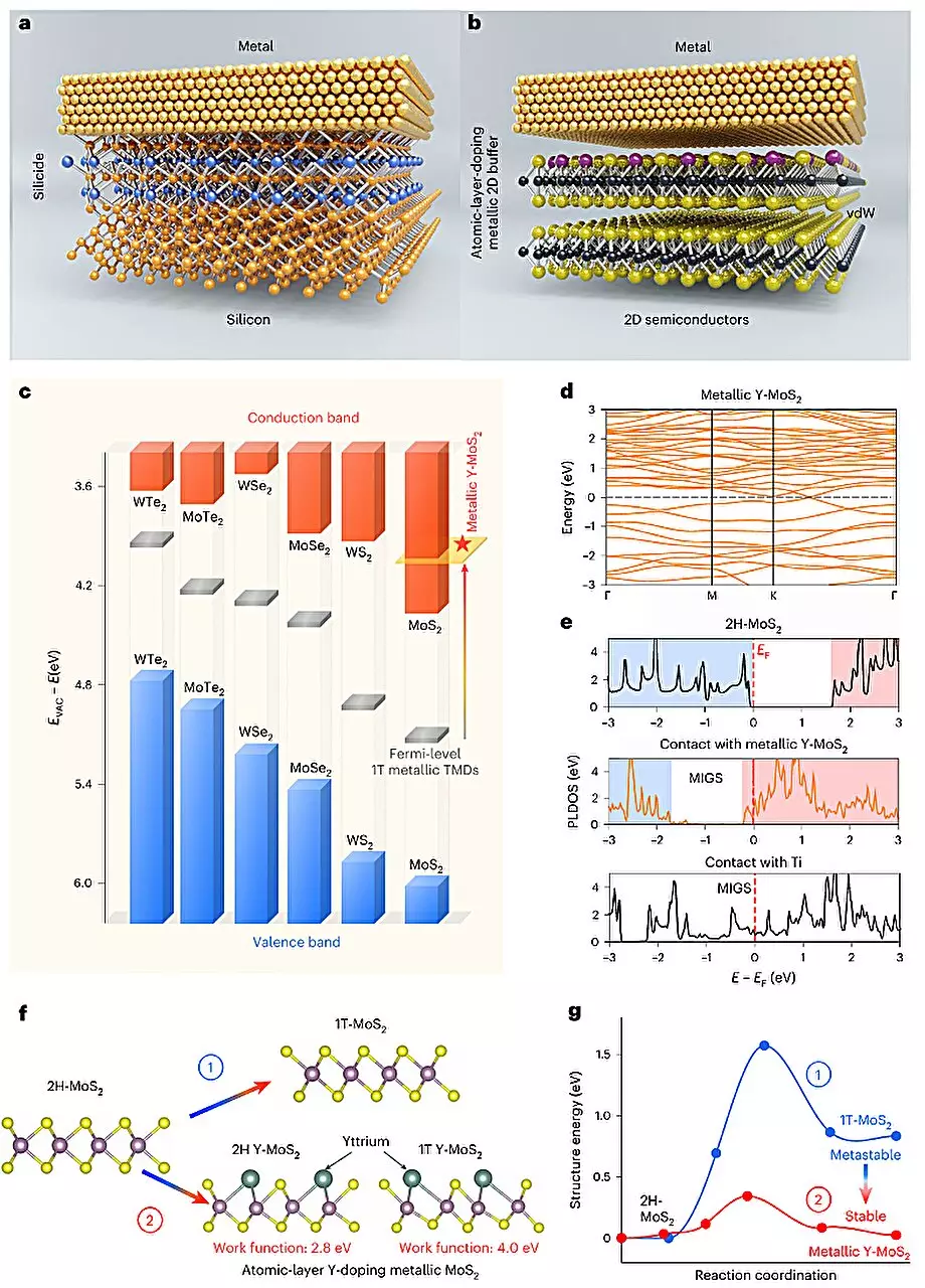
Researchers at Peking University and the Chinese Academy of Sciences have introduced a groundbreaking yttrium-doping strategy to address the issue of Fermi-level pinning effects in 2D semiconductors. By converting semiconducting molybdenum disulfide (MoS2) into metallic MoS2, this innovative approach aims to improve band alignment and enable the fabrication of ohmic contacts for 2D transistors.
The Plasma-Deposition-Annealing (PDA) Method
The team led by Chenguang Qiu developed the plasma-deposition-annealing (PDA) method to achieve yttrium doping in the surface layer of MoS2. This process involves treating patterned local contact areas with low-power soft plasma to create active sites, followed by the deposition of a Y/Ti/Au stacked metal. The 1 nm-thick active metal Y serves as a solid-state doping source, with the Y atoms diffusing into the active sites and subsequently being activated through high-temperature annealing.
The Phase Transition and Breakthrough
The researchers introduced the concept of “rare earth element yttrium doping-induced 2D phase transition” in their paper. This phase transition signifies the metallization observed when applying the yttrium doping strategy to MoS2. By inventing a selective-area single-atomic-layer surface doping technique, the team was able to achieve a remarkable doping depth of 0.5 nanometers, surpassing traditional engineering limitations.
The Future of 2D Semiconductor Integration
Through their yttrium-doping strategy, Qiu and his colleagues developed ultra-short MoS2-based channel ballistic transistors with exceptional performance as ohmic contacts and superior switching capabilities. These advancements pave the way for the development of sub-1 nanometer node chips that can deliver remarkable performance while minimizing power consumption. The researchers are now focused on creating equally impressive p-type ohmic contacts suitable for 2D semiconductors to further propel the field of electronics engineering.
Leave a Reply